
Thin films and coatings (from a few nm to about 1 µm thick) need to be optimised both in the mechanical properties and tribological performance. Typically, this is done with a combination of indentation and scratch tests. Conventional scratch test conditions are not appropriate for these types of materials as they were developed for testing thicker coatings. Instead the nano-scratch & wear module can provide what is needed.
How it works
The sample to be tested is moved perpendicular to the scratch probe whilst the contact is either held constant or ramped at a user-defined rate. Throughout the test the probe penetration depth and lateral (frictional) load are continuously monitored. Single and multi-pass tests are possible. Multi-pass tests allow the investigation of nano-wear and micro-wear.
The Nano-Scratch & Wear module has found many applications in sectors as diverse as optical, microelectronics, polymer/biomaterial, and tribological coatings. It is available as a stand alone instrument (nano-scratch tester) or as an option for the NanoTest Vantage platform.
Ramped scratch, corrected for baseline sample topography
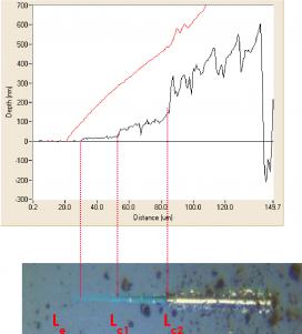
Figure 2 shows a scratch test with 3 µm end radius probe scanning over a 150 µm track at a scan speed of 2 µm/s.
A pre-scratch scan was carried out using an ultra low contact force in order to assess baseline sample topography.
The red line shows the on-load probe depth, which represents elastic and plastic depth. After 20 µm the load is ramped at 2.5 mN/s.
The black line shows the residual (plastic) depth once the scratch load has been removed. This has been corrected for initial sample topography.
The frictional force on the indenter can be recorded throughout the experiment.
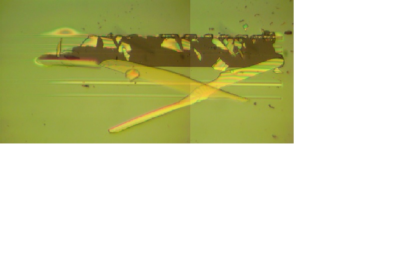
Statistically distributed nano-scratch Testing
This technique is useful where greater sensitivity to adhesion than is possible using a standard nano-scratch test is required. It has, for example, been used to investigate the situation shown in the image below:
optical coatings produced when there was a substrate cleaning problem in coating deposition
Micro-scratch Testing
The 30 N high load head can be used across the full load range for micro-scratch and micro-wear testing. The frictional force on the indenter can also be recorded throughout the entire load range.
This high load scratch capability is available on NanoTest Vantage and NanoTest Xtreme instruments equipped with the high load head.
Check out our high temperature micro-scratch and impact testing tech note which describes case studies that combine the proven NanoTest high temperature capability with micro-scale scratch and impact tests on hard, wear-resistant coatings.